
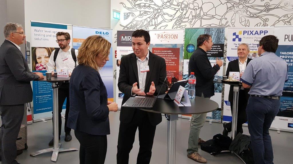
LAMpAS at EPIC Meeting on Wafer Level Optics
LAMpAS H2020 Project was one of the supporters of the EPIC Meeting on Wafer Level Optics at SUSS MicroOptics on 7-8 Nov in Neuchâtel, Switzerland. The meeting was attended by more than 100+ delegates to discuss the benefits and motivation of migrating towards wafer level manufacturing of optical diffractive, refractive or reflective components. Some of the key participants held very insightful presentations and discussions with the main goal of discussing applications in CMOS image sensors, automotive lighting, AR/VR headsets, medical, datacom, consumer electronics etc. between technology providers, system integrators and users. Some manufacturing processes were also discussed including large area master fabrication using a step and repeat UV-NIL (ultra-violet nanoimprint lithography) systems, the working stamp material and its fabrication. There was plenty of time for participants to network and collaborate for future partnerships. For more details on the event, visit HERE.